Author: Huihui Duan, Chaonan Chen, Au Group ElectronicsDec. 2008
Au Group ElectronicsThe Microchip PICkit2 is a USB based ICSP (In Circuit Serial Programming) programmer. Since its first release, Microchip has opened all resource of PICkit2 to the public, which includes all software source code and hardware schematics. With this open-architecture, DIY fans and experts can add hardware features, fix bugs, or modify the source code for operation systems other than Microsoft Windows, e.g. Linux.
PICkit2, MPLAB, ICD2, ICD3, RealICE and PICkit 2 programmer are trademarks of Microchip Technology Inc.
Note: This documents reflect only personal opinions and experiences, it shall not be used for any other purpose other than open-source/education purpose.
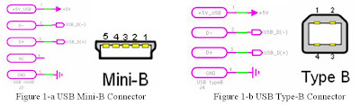
Fundamental Design of Microchip PICkit 21.1 USB Power Supply and ConnectionPICkit 2 is a USB powered device, it gets all the power from PC USB +5V power supply. In default, USB Mini-B connector (Figure 1-a) is used. However, other types of USB connectors can also be used, e.g. USB Type B connector (Figure 1-b).
The USB specification provides a 5 V supply on a single wire from which connected USB devices may draw power. The specification provides for no more than 5.25 V and no less than 4.75 V (5 V±5%) between the positive and negative bus power lines.
A USB "unit load" is defined as
100mA in USB 2.0, and was raised to
150mA in USB 3.0. A maximum of
5 unit loads can be drawn from a port in USB 2.0, and was raised to 6 in USB 3.0. There are two types of devices: low-power and high-power. Low-power devices draw at most 1 unit load, with minimum operating voltage of
4.4V in USB 2.0, and
4V in USB 3.0. High-power devices draw the maximum number of unit loads supported by the standard. All devices default as low-power but the device's software may request high-power as long as the power is available on the providing bus.
The PICkit 2 is a low-power device. Its USB current limit is set at 100mA. When the total current for both target and the PICkit 2 programmer exceeds this current limit, the USB port may turn off. In this case, the target need be powered externally.
Since PICKit 2 itself can draw electrical current as high as 75mA, the current draw for the application circuit should be limited to 25mA if PICkit 2 programmer supplies power. It is always a good practice to use external power when programming hi-performance/power-hungry chipsets, such as: dsPIC30Fs (they normally consume high current when running at high speed).
When a PICkit 2 is used to power application circuit, ensure that the application circuit does not slow the Vdd rise-time to longer than 500 us.
The +5V USB power supply is connected to capacitor C5 and C6 internally (Figure 2-a) for local voltage stability control. A 2.7Kohm resistor R34 was added after the PICKit 2 "red button" revision. R34 is used to bleed capacitor C5 and C6 when a USB connection is off. This helps improving the PICkit 2 HID-recognition performance when it is re-connected to PC in a very short interval.
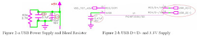
PIC18F2550 (USB microcontroller) is the soul of the PICkit 2. Two pins (D+ and D-) of PIC18F2550 are used to connect to USB Data+ and Data- from PC (Figure 2-b). All PC application program communicate with PIC18F2550 via these USB D+/D- connection.
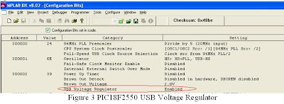
An internal 3.3V regulator is used to power the internal transceiver. A 0.47uF capacitor C7 (Figure 2-b) is used to stabilize the 3.3V supply. For PICkit 2 DIY (Do-It-Yourself), the "USB Voltage Regulator" configuration bit for PIC18F2550 must be set as "Enabled" (Figure 3).
 1.2 PIC18F2550 ICSP Connection
Like any other PIC microcontroller, the PIC18F2550 is able to be re-programmed even when it is soldered on the printed circuit board. The 5-pin ICSP connection is illustrated in figure 4-a and figure 4-b. This design provides the reprogramming and recovering capability on the chipset whenever there is anything messed up with the PICkit 2 firmware. To reprogram or recover the PIC18F2550 in the PICkit 2, another functional PIC programmer, such as PICkit 2, ICD2, ICD3, RealICE, etc. is needed. It is always a good practice to have at least two PIC programmers, e.g. one ICD2 and one PICkit 2, or two PICKit 2.
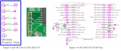
PIC18F2550 ICSP Pins
1.3 PICkit 2 ICSP VPP Boost voltage Generation and Control MechanismAs a universal PIC programmer, the VPP signal generation circuit on PICkit 2 must cover all PIC microcontrollers. The VPP voltage requirement varies from 3.3V (dsPIC33F) to 13V (PIC18F); the VPP electrical current specification is normally less than 10mA. PICkit 2 itself runs at 5 volt. Thus, an on-board switch mode boost circuit (Figure 5) is used to generate any voltage higher than target voltage ("+V_TGT" and "VDD_TGT_OUTPUT" (Figure 6-b)).
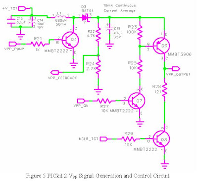
To stabilize the power supply of the switch mode boost circuit and damp the possible power noise sending back to the main power supply, C13 and C14 is used, and they should be placed as close as possible to inductor L1. The PIC18F2550 controls the switch frequency and dwell time of Q4 (both MMBT2222 (600mA) and MMBT3904 (200mA) can be used.). For DIY user, the capacity for inductor L1 should be at least 10mA. When Q4 is on, electric current flow through L1 and Q4, energy is stored in L1. When Q4 is turned off, a high voltage is generated at pin 2 of L1. The Schottky diode D3 will be on when the induced voltage is higher than the voltage on capacitor C15, electric current will keep flowing through L1 and D3. This will charge the capacitor and raise its voltage to desired VPP voltage. Resistor R22 and R24 generate a feedback signal which is send back to PIC18F2550. With "VPP_FEEDBACK" signal, the PIC18F2550 can then precisely adjust switch frequency and dwell time on Q4. This feedback boost circuit mechanism can generate a voltage higher than "VDD_TGT_OUTPUT". A large value and high voltage rated capacitor should be used as C15. R22 and R24 should use 1% or better accuracy resistor. A Schottky type diode must be used at D3 to secure low voltage drop and power consuming.
R23, R25, R27, Q7 and Q6 are used as ON/OFF switch of VPP. When "VPP_ON" is set high logic by PIC18F2550, Q7 will be on, which will then turn on Q6, the voltage on C15 will appear on PICkit 2 ICSP VPP Pin. When a low logic is send to Q7 by PIC18F2550, Q7 and Q6 will be turned off. This in turn cut off the VPP supply to external circuit. When Q6 and Q8 are both off, the PICkit 2 ICSP VPP Pin is floating. The PIC18F2550 can turn on Q8 and it will clamp PICkit 2 ICSP VPP Pin to ground. This has been used in PICkit 2 self test procedure. The overall VPP control procedure makes it possible to turn on and turn off VPP at any time.
1.4 PICkit 2 ICSP Vdd Generation and Isolation MechanismPICkit 2 can provide Vdd to power external circuit or isolate the internal generated Vdd from the external Vdd when external Vdd is detected.
On Figure 6-a, the PIC18F2550 will control the PWM dwell time of "VDD_TGT_ADJ" output, which is integrated by capacitor C8 and resistor R4. A reference voltage is generated at the negative input (U2-pin-3) of a rail to rail operational amplifier U2. R5 and R6 is used to generate voltage feedback to positive input of U2. R7 is used to generate a small electric load and bleed the capacitor (e.g. C11 and C12) when power is turned off. MOSFET Q1 is controlled by U2 in switch mode. When "+V_TGT" is lower than the voltage PIC18F2550 set, feedback voltage on U2-pin-1 is less than voltage on U2-pin-3, the output on U2-pin-4 is Low, MOSFET Q1 will turn on, the "+V_TGT" will increase. When "+V_TGT" increased to high enough to trigger U2-pin-4 to output a High logic, Q1 will be off. When Q1 is off, the "+V_TGT" will stop rising.
Overall, The PIC18F2550 set a target voltage at U2-pin3 by outputting a PWM wave, then the hardware loop of R5, R6, U2-pin-1, U2-pin-4 and Q1 automatically adjust and generate a stable output of "+V_TGT" at all load. This step-down circuit can output a 2.5V to 5V "+V_TGT" for internal and external circuits. For DIY user, U2 must be a rail-to-rail type operational amplifier; and Q1 must be a MOSFET to keep a very low voltage drop.
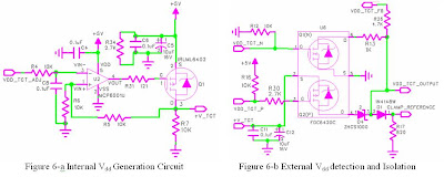
Capacitor C11 and C12 (Figure 6-b) is used to stable the "+V_TGT" for transient response. U6-Q2 (P) is used to turn on/off "+V_TGT" and isolate "+V_TGT" from "VDD_TGT_OUTPUT". When "VDD_TGT_P" output from PIC18F2550 is High (default), U6-Q2 (P) is off, no internally generated "+V_TGT" will be output to "VDD_TGT_OUTPUT". When "VDD_TGT_P" output from PIC18F2550 changes to Low, U6-Q2 (P) is on, PICKit 2 supplies Vdd to external circuits.
For protection purpose, D4 is also used to isolate internal generated Vdd with external circuit Vdd. This protection mechanism is implemented just in case anyone turns on external power supply while PICkit 2 is supplying power to external circuit. A high current Schottky type diode must be used at D4. Due to the voltage drop on D4, the maximum Vdd after D4 is around 4.8~4.9V when USB supply is 5V. Use other type of diode or small current Schottky type diode at D4 will lead to higher voltage drop. This is critical for some PIC chipset which requires a minimum Vdd 4.6V for good ICSP programming practice (an alternative approach is: always use external Vdd for those PIC chipset).
R12, R13, U6-Q1 (N) and R26 are used to detect external power supply. When the "VDD_TGT_N" output from PIC18F2550 is High logic, U6-Q1 (N) is turned on, the "VDD_TGT_FB" input to PIC18F2550 will read Low if there is no external Vdd exist, otherwise, the "VDD_TGT_FB" will read High. Every time, before connecting PICKit 2 internal Vdd to external circuit, PICkit 2 will automatically detect if external Vdd exist or not, if it does or when status is changed, a warning will be displayed.
Diode D1 and Resistor R17 generate a clamping voltage reference for PICKit 2 PGD PGC and AUX signal. Resistor R17 creates some electric load and make sure there is enough electric current flow through D1. D1 will generate some voltage drop across pin 1 and pin 2, this will compensate the Vbe voltage drop on Q2, Q3 and Q5 (MMBT3906) (Figure 7-a, 7-b, 7-c).
1.5 PICkit 2 ICSP PGD, PGC, AUX Signal Generation and Voltage Clamping MechanismPer ICSP definition, the PGC is an output only signal, PGD is a bi-direction signal. The AUX is not used for ICSP, but can be used as bi-direction signal too. Theoretically those three pins can all be used as bi-directional function. However, due to the fact the PIC18F2550 pin RA2 (PGD) and pin RA3 (PGC) are TTL type I/O, pin RA4 (AUX) are
ST type I/O. When Vdd is less than 3.6V, any operation involved with RA4 will not function correctly when TTL type input/output logic is needed. This has post some Vdd limit to some 3.3V only 11LC, 24LC EEPROM devices. Au Group Electronics developed 3-in-1 and 2-in-1
mini-labs include level-shift circuits to overcome this design limit.
Besides Programming EEPROMs and PICs, PICKit 2 can also be used as many other purpose, e.g. a Logic Tool, a UART Tool, etc.
As we have seen, the PIC18F2550 itself is working with a +5V supply, it can work directly with any +5V capable target PIC chips.
However there are more and more target PIC chips don't support +5V supply anymore, e.g. some of them can only work with voltage/signal at 3.3V, 2.7V etc.
It is a challenge job to have these PIC chips covered by PICkit 2. This technical challenge has been solved by some simple voltage level clamping technology as shown on Figure 7-a, 7-b, 7-c.
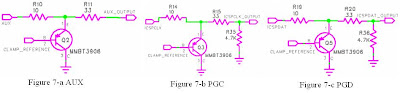
On figure 6-b, a voltage reference "CLAMP_REFERENCE" is generated by diode D1 and Resistor R17. It has been used to control the base (pin 2) on PNP transistor Q2, Q3, and Q5 (MMBT3906, Figure 7-a, 7-b, 7-c). Whenever a PIC18F2550 output a high logic (at pin AUX, ICSPCLK, ICSPDAT), and ICSP Vdd is not +5V, the Q2, Q3 and Q5 will kick-in and clamp the output voltage to Vdd level. Due to the fact there is always a voltage drop Vbe between base and emitter of transistor MMBT3906, a diode D1 is used in figure 6-b to compensate this voltage drop.
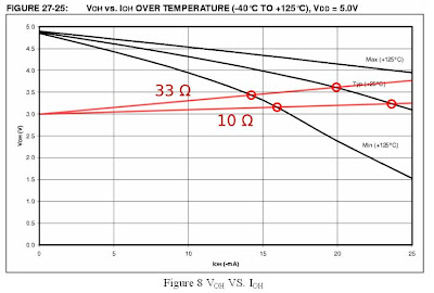
Resistors R10, R14 and R19 are used to limit the current draw from the PIC18F2550. Due to the fact VOH will drop when IOH increase (Figure 8), pin AUX (RA4), pin ICSPCLK (RA3) and pin ICSPDAT (RA2) will all be working within its safe zone.
 1.6 PICkit 2 Human Machine Interface
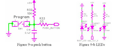
One push button (Figure 9-a) and three LEDs (Figure 9-b) are used in PICkit 2 as human machine interface. A 10K resistor R32 is used as pull-up, when there is no push button action, a logic High will send to PIC18F2550. When the "Program" push button SW1 is pushed, a logic Low will send to PIC18F2550. The push button is used to force PIC18F2550 enter bootloader mode at power-up, or trigger chip programming after power-up. The "POWER" LED will be constantly lit when PICkit 2 is power up. The "TARGET" LED will lit when PICKit 2 supply Vdd to external circuits. The "BUSY" LED will lit when PICkit2 is communicating with PC or programming a chip. Resistors R1, R2, and R3 are used to limit the current to LEDs. For DIY user, it depends the LED type you are using, any resistor between 300 ohm to 1.5K ohm should work. Using smaller value resistor, you got brighter LED but the PICKit 2 will consume more electric current.
 1.7 PICkit 2 I2C EEPROM for Programmer-To-Go (PTG) feature
PICkit 2 supports 128K byte of I2C EEPROM and 256K byte of EEPROM. Default is 128K byte of EEPROM, customer can upgrade to 256K byte of EEPROM by replace the 2 pieces of 24LC512 chipsets with 24LC1025. There is some hardware change on pin A2 between 24LC512 and 24LC1025. For DIY user, Figure 10 illustrates a hardware design to be compatible with both 24LC512 and 24LC1025. With 24LC512 on board, R38 and R39 provide pull-down connection. With 24LC1025 on board, R40 and R41 provide pull up connection. 24LC512 and 24LC1025 are exclusive, same it true for the pull-up (R40 and R41) and pull down (R38 and R39) resistors.
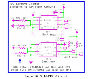
R8 and R9 provide pull up for I2C bus. PIC18F2550 store data to I2C EEPROM by SCL and SDA connection. With the on board EEPROM, the PICKit 2 can program PIC microcontrollers without a PC.
1.8 PICkit 2 ICSP interfaceTwo types of ICSP interfaces are used in Microchip programmers: RJ12 6p6c connector (Figure 11-a), and 6-pin female header (0.100" spacing) (Figure 11-b). Functionally, they are identical and each has its own pros and cons. The error-proof RJ12 connector using spring contacts to compensate the worn out on pins, it is relatively expensive and takes more space on circuit board. The 6-pin female header takes less circuit board space, but there is limit compensation for pin/contact worn out and there is no mechanism to prevent backwards connection. The RJ12 connector is used in ICD2, ICD3, and RealICE. The 6-pin female header is used in PICKit 2 and PICkit 3. For DIY user, either 6-pin female header or RJ12 connector can be used. For high quality purpose, the RJ12 connector is recommended.
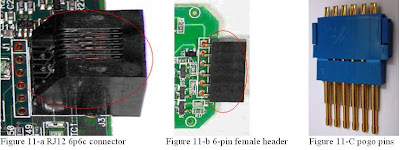
Pogo pin technology (Figure 11-C) can be used to extend the connector life for RJ12 connector and 6-pin header, it is highly recommended for heavy duty usage or manufacturing environment.
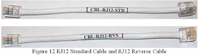
The ICSP signal definition on programmer side between the RJ12 6p6c connector and the 6pin female header is opposite. This situation can be easily solved by using different ICSP cables. For ICD2, ICD3, and RealICE, a RJ12 standard cable (Figure 12) is normally used. To be compatible with any circuit board developed for ICD2, a RJ12 reverse cable (Figure 12) can be used with Au Group Electronics developed BB0703 product family.
 References:
Special thanks for Walter Kicinski from Microchip Technology Inc. for his constant Support.
1. PICkit 2 Microcontroller Programmer User’s Guide; DS51553E 2/27/2008
2. Au Group Electronics CB0703 Schematic:
http://www.auelectronics.com/Hardware-CB0703.htm3. http://en.wikipedia.org/wiki/USB
4. Microchip PIC18F2455/2550/4455/4550 Data Sheet
5. Microchip PIC18F2220/2320/4220/4320 Data Sheet, Figure 27-25
6. Google Groups:
pickit-devel


