Author: Chaonan Chen, Huihui Duan, Au Group Electronics
We own a magicJack since May, 2008, and have been contacting with magicJack and asking them about when the Canadian phone number will be available for our customer. The answer was they were still working on this, and did not have an anticipate date yet.
Until recently, the great news come out, magicJack Canadian phone number is available now. Even though just a few provinces’ phone numbers are available to choose from, it is still good news to magicJack Canadian users.
We activated one magicJack with phone number in Windsor, Ontario area recently for our customer. And following is the step by step of the activation procedure.
1. Plug a magicJack to USB port of PC, a magicJack picture with a sentence “One minute of Patience For a lifetime of Savings” (Figure 1) will be showing on your PC
2. Wait until the magicJack interface displayed, notice that magicJack phone number is not assigned yet (000-000-0000), and click the “Click to Register” button located at the left bottom side (Figure 2).
3. Choose one of the options depends on where the magicJack was purchased. Here we I chose the 2nd option as it was purchased from Au Group Electronics, a magicJack authorized reseller, then click next (Figure 3).
4. Choose one of the options then click Next: You can create a new magicJack account no matter you already have a magicJack or not. Or you can add the new magicJack to your registered magicJack account.
The owner already have a magicJack and prefer to have all magicJack under one account/email, so chose the 2nd option, then input the owner's registered magicJack email and password to log in to the magicJack account to add the new magicJack, then click “Next”
5. Select 911 location, you can either create a new location (this new address can be set at any country, but only address in United States will be covered in 911 Emergency service ) or choose a location from the existing account
6. Fill the name, country, Zip code, State/Province, City, Street Number, Street Name, Street Type, and any additional detail like apartment #, as this information are required when placing a 911 call. The location can be changed in the future. After that, select which service are you using for television network and internet service. We chose Cable for both, then click Next (Figure 6)
7. Read and agree the Terms of Service by check the check box of “I have read and agree to the Terms of Service”, then click Next (Figure 7).
8. Select “I want a Canadian Number for $10 a year”. Then choose a Province, Area code, and Prefix. Available phone # will be listed, select a number from the list, check “I elect to accept free outgoing service”, and then click “Reserve my Number” (Figure 8).
9. Verify or edit the Billing address by click “Edit address”(figure 9)
10. Enter the billing address and credit card information (for the $10 charge), then click save (figure 10)
Sunday, December 6, 2009
Monday, June 8, 2009
AU PIC18F Serial Bootloader User Manual (Simplified)
Author: Huihui Duan, Chaonan Chen, Au Group Electronics
1 WHAT IS AU PIC18F SERIAL BOOTLOADER?
Au PIC18F Serial Bootloaders are low cost yet high reliable solutions for upgrading PIC18F Microcontroller (MCU) firmware via RS232 interfaces. They are suitable for any target boards/products equipped with Microchip® PIC18F microcontrollers and RS232 interfaces.
With the Au PIC18F bootloader program embedded in the PIC18F MCU, new application firmware code can be upgraded into PIC18F MCU in-field without bringing the device back to manufacturer’s facility. The application firmware code is downloaded via a PC RS232 interface. So there is no need to open/damage products original package/enclosure.
2 TWO SOLUTIONS
There are two solutions available for Au PIC18F serial bootloader: non-encrypted solution and encrypted solution.
• Non-encrypted solution uses regular "Hex" format files for firmware upgrade; it can be used for products with no requirements of intellectual property (IP) protection.
• Encrypted solution uses encrypted algorithm in a proprietary "Aud" format to prevent the PIC18F firmware from directly exposure to third parties. The unique dynamic encryption algorithm makes firmware-hack mission impossible. The encryption feature helps preventing the firmware intellectual property from being copied/miss-used by un-authorized third parties.
With Au Group Electronics developed encryption technology, for any encrypted solution:
1. Each encrypted firmware code (*.aud file) is unique;
2. Each encrypted firmware code (*.aud file) is traceable with a unique digital watermark;
3. Each firmware-downloading process is unique.
All these three features provide a good protection of Intellectual Property (IP).
MCU resources used for both solutions are listed in Table 1-1. Please note, EEPROM is reserved for software trigger feature.

Au Group Electronics is proud to announce the following Au Group Electronics developed products are maintained and protected by PIC18F Encrypted Serial Bootloader: six editions of J1939 Simulators, J1939 Data Centers, J1939 Message Centers, J1939 Interpreters, etc. Au Group Electronics also provide/design other PIC family bootloaders with or without encryption features, e.g. dsPIC30Fs, dsPIC33Fs, etc.
In this user manual, we will use Au J1939 Simulator Gen II as an example to demonstrate how easy an Au PIC18F Serial Bootloader can be applied to a product (Chapter 1.7).
Note: Microchip, PIC18F, PICkit 2, and ICD2 are trademark of Microchip Inc.
3 MAJOR FEATURES OF AU PIC18F SERIAL BOOTLOADER
The following features have been tested and used in-field and are listed here:
• High Reliability
• High level of Security
• Low cost
• Turn key solution and full support
• Great flexibility: Custom design available, e.g. encrypted and non-encrypted solutions; different oscillator frequencies, 20M Hz, 16M Hz, etc.; different communication baud Rate: 115.2K, 57.6K, etc.
Au PIC18F serial bootloader is also been considered as a "Green" product for the following features:
• No need to take the circuit board out of the enclosure. So the product package won’t be damaged. (Save material and time)
• No extra programming tool or software needed. (Save tooling cost)
• No need to send final products to original manufacturer. (Save shipping cost and time)
• No more long waiting period (e.g. days, weeks) while product is being upgraded. It only takes from a few seconds to a few minutes to upgrade the product. (Save time)
4 WHAT'S NEEDED TO USE AU PIC18F SERIAL BOOTLOADER?
Following items are needed to use Au bootload firmware with a PIC18F MCU:
1. Customer application hardware (e.g. circuit board, devices, etc.) with PIC18F microcontroller and RS232 interface
2. Customer application software (in hex format or aud format)
3. Bootloader hex code: e.g. an Au PIC18F4580 Bootloader
4. MCU programmer: e.g. Au BB0703 (PICkit 2) family products
5. RS232 extension cable: connect to RS232 port on PC
6. USB cable: to connect a PC to MCU programmer (BB0703)
7. USB to RS232 converter: optional, it is only needed for PC only equipped with USB ports
Note: Due to the fact, few serial ports are available in modern computers, Au PIC18F serial bootloader is designed to be compatible with most popular USB to RS232 converters. All Au PIC18F serial bootloader products have been rigorously tested with regular PC serial ports and USB to RS232 converters.
8. PC with RS232 port and USB port. Also the following software are needed:
a. Au PIC18F Serial Bootloader PC side application software
b. PIC Programmer PC side software: e.g. PICKit 2 Programmer
c. Microcontroller development software: e.g. MPLAB IDE, MCU C compiler
d. Hex encryption PC side software: Au HexEncoder (Optional)
Item 1, 2, 4, 5, 6, 7 are customer provided or designed items. Item 3, 8-a, 8-d are provided by Au Group Electronics. Item 8-b and 8-c are available from Microchip or MCU Compiler vendors.
5 RECOMMENDATION OF SERIAL INTERFACE CIRCUITS DESIGN
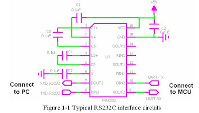
The following diagram (Figure 1-1) illustrates a typical RS232C interface circuit for application design.
6 INFORMATION NEEDED FROM CUSTOMER
To get custom designed PIC18F bootloader started, the following information is needed:
1. Particular PIC18F controller model, package
2. Microcontroller oscillator frequency
3. Microcontroller oscillator mode
4. Bootloader hardware trigger pin assignment
5. Bootloader mode LED assignment
6. Other special configuration bits requirements
7. Optional software bootloader entry trigger feature: If software bootloader entry trigger feature is needed, more application memory space will be needed. This also requires some customer program for the integration.
7 ITEMS CUSTOMER WILL RECEIVE
1. A CD includes the following items:
a. Au PIC18F bootloader hex code (*.hex).
b. A PC installation program for Au PIC bootloader application software
c. Hex Encoder (optional): a PC installation program for hex encryption. This item is only provided with the purchase of an encrypted bootloader solution.
2. User manual for Au PIC18F Serial Bootloader
8 APPLICATION EXAMPLE
Now, we will outline the procedure of how the Au PIC18F Serial Bootloader is applied in one of our products – Au J1939 Simulator (Gen II). The whole procedure is summarized in Figure 1-2.
1. At the manufacturer facility, PIC18F Serial Bootloader hex file is merged with the J1939 Simulator Application hex file.
2. Target chipset (PIC18F MCU) is soldered on PCB, 6 ICSP (In-Circuit Serial Programming) pads are available on PCB
3. Connect PC with programmer (BB0703) through a USB cable.
4. Connect BB0703 with the target board through an Au POGO cable.
5. Merged hex file was first burned in the target PIC18F MCU by BB0703 through the POGO cable and the USB cable before the circuit board is installed into the enclosure.
6. Assemble all other components and package them into an enclosure.
7. Final products are delivered to end user/dealer/sales office
8. When new J1939 Simulator application software (firmware) needs to be upgraded, Au Group Electronics sends encrypted "aud" file to end-user/dealer/sale office by email, software disc, USB thumb drive, or FTP, etc.
9. The end-user/dealer/sales connects J1939 Simulator to a PC with a RS232 cable, then the aud file can be downloaded into PIC18F chip in-field, so the new feature is ready in a very short time (ranging from a few seconds to a few minutes).
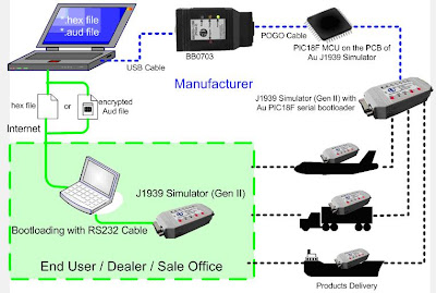
Figure 1-2 Product lifetime firmware management with Au PIC18F Serial Bootloader
This is a simlified edition of Au PIC18F Serial Bootloader User Manual, for detail information about how to merge your application software with Au Group Electronics developed PIC18F bootloader, please contact us at support@auelectronics.com
1 WHAT IS AU PIC18F SERIAL BOOTLOADER?
Au PIC18F Serial Bootloaders are low cost yet high reliable solutions for upgrading PIC18F Microcontroller (MCU) firmware via RS232 interfaces. They are suitable for any target boards/products equipped with Microchip® PIC18F microcontrollers and RS232 interfaces.
With the Au PIC18F bootloader program embedded in the PIC18F MCU, new application firmware code can be upgraded into PIC18F MCU in-field without bringing the device back to manufacturer’s facility. The application firmware code is downloaded via a PC RS232 interface. So there is no need to open/damage products original package/enclosure.
2 TWO SOLUTIONS
There are two solutions available for Au PIC18F serial bootloader: non-encrypted solution and encrypted solution.
• Non-encrypted solution uses regular "Hex" format files for firmware upgrade; it can be used for products with no requirements of intellectual property (IP) protection.
• Encrypted solution uses encrypted algorithm in a proprietary "Aud" format to prevent the PIC18F firmware from directly exposure to third parties. The unique dynamic encryption algorithm makes firmware-hack mission impossible. The encryption feature helps preventing the firmware intellectual property from being copied/miss-used by un-authorized third parties.
With Au Group Electronics developed encryption technology, for any encrypted solution:
1. Each encrypted firmware code (*.aud file) is unique;
2. Each encrypted firmware code (*.aud file) is traceable with a unique digital watermark;
3. Each firmware-downloading process is unique.
All these three features provide a good protection of Intellectual Property (IP).
MCU resources used for both solutions are listed in Table 1-1. Please note, EEPROM is reserved for software trigger feature.

Au Group Electronics is proud to announce the following Au Group Electronics developed products are maintained and protected by PIC18F Encrypted Serial Bootloader: six editions of J1939 Simulators, J1939 Data Centers, J1939 Message Centers, J1939 Interpreters, etc. Au Group Electronics also provide/design other PIC family bootloaders with or without encryption features, e.g. dsPIC30Fs, dsPIC33Fs, etc.
In this user manual, we will use Au J1939 Simulator Gen II as an example to demonstrate how easy an Au PIC18F Serial Bootloader can be applied to a product (Chapter 1.7).
Note: Microchip, PIC18F, PICkit 2, and ICD2 are trademark of Microchip Inc.
3 MAJOR FEATURES OF AU PIC18F SERIAL BOOTLOADER
The following features have been tested and used in-field and are listed here:
• High Reliability
• High level of Security
• Low cost
• Turn key solution and full support
• Great flexibility: Custom design available, e.g. encrypted and non-encrypted solutions; different oscillator frequencies, 20M Hz, 16M Hz, etc.; different communication baud Rate: 115.2K, 57.6K, etc.
Au PIC18F serial bootloader is also been considered as a "Green" product for the following features:
• No need to take the circuit board out of the enclosure. So the product package won’t be damaged. (Save material and time)
• No extra programming tool or software needed. (Save tooling cost)
• No need to send final products to original manufacturer. (Save shipping cost and time)
• No more long waiting period (e.g. days, weeks) while product is being upgraded. It only takes from a few seconds to a few minutes to upgrade the product. (Save time)
4 WHAT'S NEEDED TO USE AU PIC18F SERIAL BOOTLOADER?
Following items are needed to use Au bootload firmware with a PIC18F MCU:
1. Customer application hardware (e.g. circuit board, devices, etc.) with PIC18F microcontroller and RS232 interface
2. Customer application software (in hex format or aud format)
3. Bootloader hex code: e.g. an Au PIC18F4580 Bootloader
4. MCU programmer: e.g. Au BB0703 (PICkit 2) family products
5. RS232 extension cable: connect to RS232 port on PC
6. USB cable: to connect a PC to MCU programmer (BB0703)
7. USB to RS232 converter: optional, it is only needed for PC only equipped with USB ports
Note: Due to the fact, few serial ports are available in modern computers, Au PIC18F serial bootloader is designed to be compatible with most popular USB to RS232 converters. All Au PIC18F serial bootloader products have been rigorously tested with regular PC serial ports and USB to RS232 converters.
8. PC with RS232 port and USB port. Also the following software are needed:
a. Au PIC18F Serial Bootloader PC side application software
b. PIC Programmer PC side software: e.g. PICKit 2 Programmer
c. Microcontroller development software: e.g. MPLAB IDE, MCU C compiler
d. Hex encryption PC side software: Au HexEncoder (Optional)
Item 1, 2, 4, 5, 6, 7 are customer provided or designed items. Item 3, 8-a, 8-d are provided by Au Group Electronics. Item 8-b and 8-c are available from Microchip or MCU Compiler vendors.
5 RECOMMENDATION OF SERIAL INTERFACE CIRCUITS DESIGN
The following diagram (Figure 1-1) illustrates a typical RS232C interface circuit for application design.

6 INFORMATION NEEDED FROM CUSTOMER
To get custom designed PIC18F bootloader started, the following information is needed:
1. Particular PIC18F controller model, package
2. Microcontroller oscillator frequency
3. Microcontroller oscillator mode
4. Bootloader hardware trigger pin assignment
5. Bootloader mode LED assignment
6. Other special configuration bits requirements
7. Optional software bootloader entry trigger feature: If software bootloader entry trigger feature is needed, more application memory space will be needed. This also requires some customer program for the integration.
7 ITEMS CUSTOMER WILL RECEIVE
1. A CD includes the following items:
a. Au PIC18F bootloader hex code (*.hex).
b. A PC installation program for Au PIC bootloader application software
c. Hex Encoder (optional): a PC installation program for hex encryption. This item is only provided with the purchase of an encrypted bootloader solution.
2. User manual for Au PIC18F Serial Bootloader
8 APPLICATION EXAMPLE
Now, we will outline the procedure of how the Au PIC18F Serial Bootloader is applied in one of our products – Au J1939 Simulator (Gen II). The whole procedure is summarized in Figure 1-2.
1. At the manufacturer facility, PIC18F Serial Bootloader hex file is merged with the J1939 Simulator Application hex file.
2. Target chipset (PIC18F MCU) is soldered on PCB, 6 ICSP (In-Circuit Serial Programming) pads are available on PCB
3. Connect PC with programmer (BB0703) through a USB cable.
4. Connect BB0703 with the target board through an Au POGO cable.
5. Merged hex file was first burned in the target PIC18F MCU by BB0703 through the POGO cable and the USB cable before the circuit board is installed into the enclosure.
6. Assemble all other components and package them into an enclosure.
7. Final products are delivered to end user/dealer/sales office
8. When new J1939 Simulator application software (firmware) needs to be upgraded, Au Group Electronics sends encrypted "aud" file to end-user/dealer/sale office by email, software disc, USB thumb drive, or FTP, etc.
9. The end-user/dealer/sales connects J1939 Simulator to a PC with a RS232 cable, then the aud file can be downloaded into PIC18F chip in-field, so the new feature is ready in a very short time (ranging from a few seconds to a few minutes).

Figure 1-2 Product lifetime firmware management with Au PIC18F Serial Bootloader
This is a simlified edition of Au PIC18F Serial Bootloader User Manual, for detail information about how to merge your application software with Au Group Electronics developed PIC18F bootloader, please contact us at support@auelectronics.com
Labels:
PIC18F SERIAL BOOTLOADER
Monday, May 18, 2009
Au Hex Encoder User Manual (Rev. A, June-2008)
Author: Huihui Duan, Chaonan Chen, Au Group Electronics
Au Group Electronics provides custom designed Hex Encoder program for each individual customer who bought bootloader products with encryption feature.
Au Group Electronics Hex Encoder is a software program which converts non-encrypted hex file to encrypted Aud file with custom designed encryption algorithm. The encrypted Aud file can be used to upgrade microcontroller flash memory in-field for any products with Au Group Electronics developed bootloader technology. No non-encrypted hex will be send to the end user any more!
Note: To use encrypted Aud files, custom-made bootloader application software with specific encryption/decryption algorithm is required.
The user manual will explain how to install Au Hex Encoder step by step and how to use the Hex Encoder toolset for converting a non-encrypted hex file to an encrypted Aud file.
How to Install AU Hex Encoder
1. Double click the "Setup Au HexEncoder V1.00A" application file, as shown in Figure 1

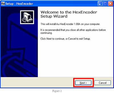
2. Click "Next" in the welcome window, as shown in Figure 2
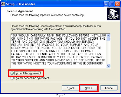
3. In License Agreement window, select "I accept the agreement", then click "Next" (Figure 3)
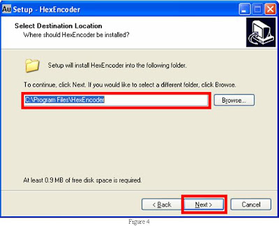
4. Select default destination location, then click "Next" (Figure 4)
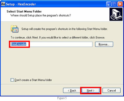
5. Use the default "HexEncoder" as Start Menu Folder, click "Next" (Figure 5)
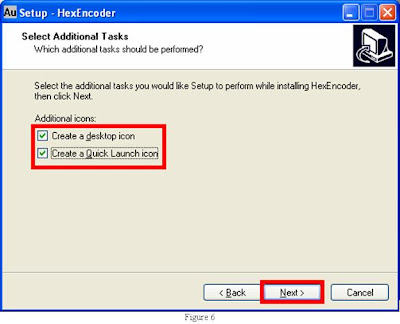
6. Check "Create a desktop Icon", and "Create a Quick Launch Icon", then click "Next" (Figure 6)
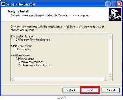
7. Click "Install" in the "Ready to Install" window (Figure 7)
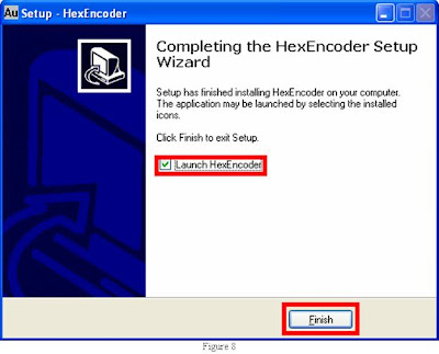
8. Check "Launch HexEncoder", click "Finish" to exit Setup (Figure 8)
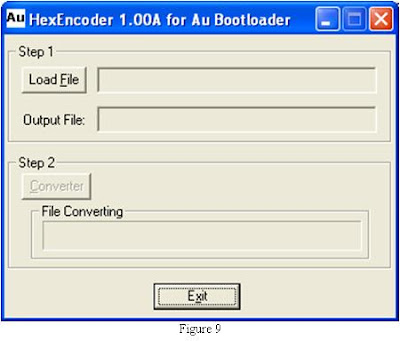
9. "HexEncoder 1.00A for Au Bootloader" window pops up (Figure 9)
How to Use AU Hex Encoder?
1. Double click "Au HexEncoder" shortcut (Figure 10) to open the software program

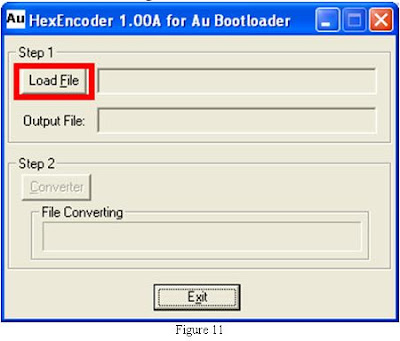
2. Click "Load File" button, as shown in Figure 11
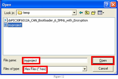
3. Select a hex file, then click "Open" (Figure 12)
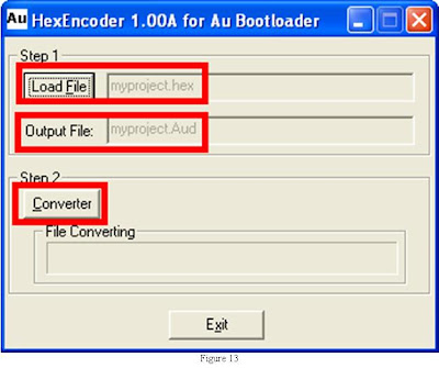
4. Loaded file is displayed after the button "Load File" in the format of "*.hex"; output file is displayed after the icon "Output File" in the format of "*.Aud", click "Converter" button (Figure 13).
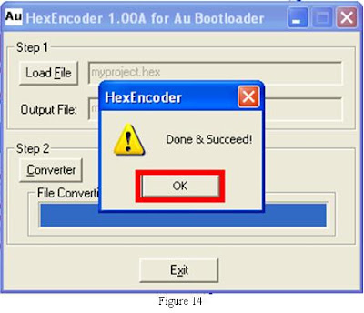
5. File converting status bar will show the process as converting proceed, and a message box "Done & Succeed!" will display upon finishing, click "OK" (Figure 14)
6. The output Aud file will be saved automatically at the same location as loaded hex file. Another *.Aux will also be generated. The Aux file is for technical support/verification purpose only. It can only be used for Au Group Electronics customer technology support purpose. (Figure 15).

7. Click "Load File" and repeat above step 3 to step 6 to convert another hex file, otherwise, click "Exit" to close the HexEncoder application program (Figure 16).

Au Group Electronics provides custom designed Hex Encoder program for each individual customer who bought bootloader products with encryption feature.
Au Group Electronics Hex Encoder is a software program which converts non-encrypted hex file to encrypted Aud file with custom designed encryption algorithm. The encrypted Aud file can be used to upgrade microcontroller flash memory in-field for any products with Au Group Electronics developed bootloader technology. No non-encrypted hex will be send to the end user any more!
Note: To use encrypted Aud files, custom-made bootloader application software with specific encryption/decryption algorithm is required.
The user manual will explain how to install Au Hex Encoder step by step and how to use the Hex Encoder toolset for converting a non-encrypted hex file to an encrypted Aud file.
How to Install AU Hex Encoder
1. Double click the "Setup Au HexEncoder V1.00A" application file, as shown in Figure 1

2. Click "Next" in the welcome window, as shown in Figure 2

3. In License Agreement window, select "I accept the agreement", then click "Next" (Figure 3)

4. Select default destination location, then click "Next" (Figure 4)

5. Use the default "HexEncoder" as Start Menu Folder, click "Next" (Figure 5)

6. Check "Create a desktop Icon", and "Create a Quick Launch Icon", then click "Next" (Figure 6)

7. Click "Install" in the "Ready to Install" window (Figure 7)

8. Check "Launch HexEncoder", click "Finish" to exit Setup (Figure 8)

9. "HexEncoder 1.00A for Au Bootloader" window pops up (Figure 9)

How to Use AU Hex Encoder?
1. Double click "Au HexEncoder" shortcut (Figure 10) to open the software program

2. Click "Load File" button, as shown in Figure 11

3. Select a hex file, then click "Open" (Figure 12)

4. Loaded file is displayed after the button "Load File" in the format of "*.hex"; output file is displayed after the icon "Output File" in the format of "*.Aud", click "Converter" button (Figure 13).

5. File converting status bar will show the process as converting proceed, and a message box "Done & Succeed!" will display upon finishing, click "OK" (Figure 14)

6. The output Aud file will be saved automatically at the same location as loaded hex file. Another *.Aux will also be generated. The Aux file is for technical support/verification purpose only. It can only be used for Au Group Electronics customer technology support purpose. (Figure 15).

7. Click "Load File" and repeat above step 3 to step 6 to convert another hex file, otherwise, click "Exit" to close the HexEncoder application program (Figure 16).

Labels:
Au Hex Encoder
Monday, May 11, 2009
Understanding Microchip PICkit 2 Hardware (Rev. A)
Author: Huihui Duan, Chaonan Chen, Au Group Electronics
Dec. 2008
Au Group Electronics
The Microchip PICkit2 is a USB based ICSP (In Circuit Serial Programming) programmer. Since its first release, Microchip has opened all resource of PICkit2 to the public, which includes all software source code and hardware schematics. With this open-architecture, DIY fans and experts can add hardware features, fix bugs, or modify the source code for operation systems other than Microsoft Windows, e.g. Linux.
PICkit2, MPLAB, ICD2, ICD3, RealICE and PICkit 2 programmer are trademarks of Microchip Technology Inc.
Note: This documents reflect only personal opinions and experiences, it shall not be used for any other purpose other than open-source/education purpose.
Fundamental Design of Microchip PICkit 2
1.1 USB Power Supply and Connection
PICkit 2 is a USB powered device, it gets all the power from PC USB +5V power supply. In default, USB Mini-B connector (Figure 1-a) is used. However, other types of USB connectors can also be used, e.g. USB Type B connector (Figure 1-b).

The USB specification provides a 5 V supply on a single wire from which connected USB devices may draw power. The specification provides for no more than 5.25 V and no less than 4.75 V (5 V±5%) between the positive and negative bus power lines.
A USB "unit load" is defined as 100mA in USB 2.0, and was raised to 150mA in USB 3.0. A maximum of 5 unit loads can be drawn from a port in USB 2.0, and was raised to 6 in USB 3.0. There are two types of devices: low-power and high-power. Low-power devices draw at most 1 unit load, with minimum operating voltage of 4.4V in USB 2.0, and 4V in USB 3.0. High-power devices draw the maximum number of unit loads supported by the standard. All devices default as low-power but the device's software may request high-power as long as the power is available on the providing bus.
The PICkit 2 is a low-power device. Its USB current limit is set at 100mA. When the total current for both target and the PICkit 2 programmer exceeds this current limit, the USB port may turn off. In this case, the target need be powered externally.
Since PICKit 2 itself can draw electrical current as high as 75mA, the current draw for the application circuit should be limited to 25mA if PICkit 2 programmer supplies power. It is always a good practice to use external power when programming hi-performance/power-hungry chipsets, such as: dsPIC30Fs (they normally consume high current when running at high speed).
When a PICkit 2 is used to power application circuit, ensure that the application circuit does not slow the Vdd rise-time to longer than 500 us.
The +5V USB power supply is connected to capacitor C5 and C6 internally (Figure 2-a) for local voltage stability control. A 2.7Kohm resistor R34 was added after the PICKit 2 "red button" revision. R34 is used to bleed capacitor C5 and C6 when a USB connection is off. This helps improving the PICkit 2 HID-recognition performance when it is re-connected to PC in a very short interval.

PIC18F2550 (USB microcontroller) is the soul of the PICkit 2. Two pins (D+ and D-) of PIC18F2550 are used to connect to USB Data+ and Data- from PC (Figure 2-b). All PC application program communicate with PIC18F2550 via these USB D+/D- connection.
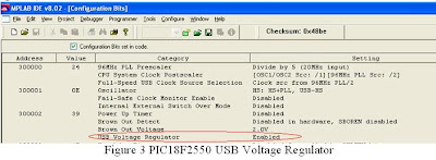
An internal 3.3V regulator is used to power the internal transceiver. A 0.47uF capacitor C7 (Figure 2-b) is used to stabilize the 3.3V supply. For PICkit 2 DIY (Do-It-Yourself), the "USB Voltage Regulator" configuration bit for PIC18F2550 must be set as "Enabled" (Figure 3).
1.2 PIC18F2550 ICSP Connection
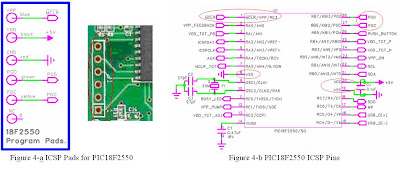
Like any other PIC microcontroller, the PIC18F2550 is able to be re-programmed even when it is soldered on the printed circuit board. The 5-pin ICSP connection is illustrated in figure 4-a and figure 4-b. This design provides the reprogramming and recovering capability on the chipset whenever there is anything messed up with the PICkit 2 firmware. To reprogram or recover the PIC18F2550 in the PICkit 2, another functional PIC programmer, such as PICkit 2, ICD2, ICD3, RealICE, etc. is needed. It is always a good practice to have at least two PIC programmers, e.g. one ICD2 and one PICkit 2, or two PICKit 2.
As a universal PIC programmer, the VPP signal generation circuit on PICkit 2 must cover all PIC microcontrollers. The VPP voltage requirement varies from 3.3V (dsPIC33F) to 13V (PIC18F); the VPP electrical current specification is normally less than 10mA. PICkit 2 itself runs at 5 volt. Thus, an on-board switch mode boost circuit (Figure 5) is used to generate any voltage higher than target voltage ("+V_TGT" and "VDD_TGT_OUTPUT" (Figure 6-b)).
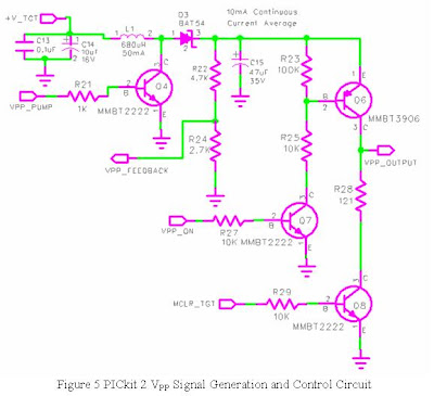
To stabilize the power supply of the switch mode boost circuit and damp the possible power noise sending back to the main power supply, C13 and C14 is used, and they should be placed as close as possible to inductor L1. The PIC18F2550 controls the switch frequency and dwell time of Q4 (both MMBT2222 (600mA) and MMBT3904 (200mA) can be used.). For DIY user, the capacity for inductor L1 should be at least 10mA. When Q4 is on, electric current flow through L1 and Q4, energy is stored in L1. When Q4 is turned off, a high voltage is generated at pin 2 of L1. The Schottky diode D3 will be on when the induced voltage is higher than the voltage on capacitor C15, electric current will keep flowing through L1 and D3. This will charge the capacitor and raise its voltage to desired VPP voltage. Resistor R22 and R24 generate a feedback signal which is send back to PIC18F2550. With "VPP_FEEDBACK" signal, the PIC18F2550 can then precisely adjust switch frequency and dwell time on Q4. This feedback boost circuit mechanism can generate a voltage higher than "VDD_TGT_OUTPUT". A large value and high voltage rated capacitor should be used as C15. R22 and R24 should use 1% or better accuracy resistor. A Schottky type diode must be used at D3 to secure low voltage drop and power consuming.
R23, R25, R27, Q7 and Q6 are used as ON/OFF switch of VPP. When "VPP_ON" is set high logic by PIC18F2550, Q7 will be on, which will then turn on Q6, the voltage on C15 will appear on PICkit 2 ICSP VPP Pin. When a low logic is send to Q7 by PIC18F2550, Q7 and Q6 will be turned off. This in turn cut off the VPP supply to external circuit. When Q6 and Q8 are both off, the PICkit 2 ICSP VPP Pin is floating. The PIC18F2550 can turn on Q8 and it will clamp PICkit 2 ICSP VPP Pin to ground. This has been used in PICkit 2 self test procedure. The overall VPP control procedure makes it possible to turn on and turn off VPP at any time.
1.4 PICkit 2 ICSP Vdd Generation and Isolation Mechanism
PICkit 2 can provide Vdd to power external circuit or isolate the internal generated Vdd from the external Vdd when external Vdd is detected.
On Figure 6-a, the PIC18F2550 will control the PWM dwell time of "VDD_TGT_ADJ" output, which is integrated by capacitor C8 and resistor R4. A reference voltage is generated at the negative input (U2-pin-3) of a rail to rail operational amplifier U2. R5 and R6 is used to generate voltage feedback to positive input of U2. R7 is used to generate a small electric load and bleed the capacitor (e.g. C11 and C12) when power is turned off. MOSFET Q1 is controlled by U2 in switch mode. When "+V_TGT" is lower than the voltage PIC18F2550 set, feedback voltage on U2-pin-1 is less than voltage on U2-pin-3, the output on U2-pin-4 is Low, MOSFET Q1 will turn on, the "+V_TGT" will increase. When "+V_TGT" increased to high enough to trigger U2-pin-4 to output a High logic, Q1 will be off. When Q1 is off, the "+V_TGT" will stop rising.
Overall, The PIC18F2550 set a target voltage at U2-pin3 by outputting a PWM wave, then the hardware loop of R5, R6, U2-pin-1, U2-pin-4 and Q1 automatically adjust and generate a stable output of "+V_TGT" at all load. This step-down circuit can output a 2.5V to 5V "+V_TGT" for internal and external circuits. For DIY user, U2 must be a rail-to-rail type operational amplifier; and Q1 must be a MOSFET to keep a very low voltage drop.
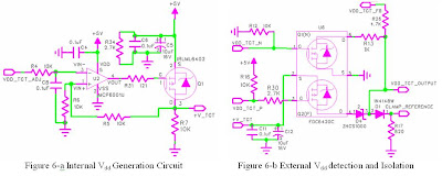
Capacitor C11 and C12 (Figure 6-b) is used to stable the "+V_TGT" for transient response. U6-Q2 (P) is used to turn on/off "+V_TGT" and isolate "+V_TGT" from "VDD_TGT_OUTPUT". When "VDD_TGT_P" output from PIC18F2550 is High (default), U6-Q2 (P) is off, no internally generated "+V_TGT" will be output to "VDD_TGT_OUTPUT". When "VDD_TGT_P" output from PIC18F2550 changes to Low, U6-Q2 (P) is on, PICKit 2 supplies Vdd to external circuits.
For protection purpose, D4 is also used to isolate internal generated Vdd with external circuit Vdd. This protection mechanism is implemented just in case anyone turns on external power supply while PICkit 2 is supplying power to external circuit. A high current Schottky type diode must be used at D4. Due to the voltage drop on D4, the maximum Vdd after D4 is around 4.8~4.9V when USB supply is 5V. Use other type of diode or small current Schottky type diode at D4 will lead to higher voltage drop. This is critical for some PIC chipset which requires a minimum Vdd 4.6V for good ICSP programming practice (an alternative approach is: always use external Vdd for those PIC chipset).
R12, R13, U6-Q1 (N) and R26 are used to detect external power supply. When the "VDD_TGT_N" output from PIC18F2550 is High logic, U6-Q1 (N) is turned on, the "VDD_TGT_FB" input to PIC18F2550 will read Low if there is no external Vdd exist, otherwise, the "VDD_TGT_FB" will read High. Every time, before connecting PICKit 2 internal Vdd to external circuit, PICkit 2 will automatically detect if external Vdd exist or not, if it does or when status is changed, a warning will be displayed.
Diode D1 and Resistor R17 generate a clamping voltage reference for PICKit 2 PGD PGC and AUX signal. Resistor R17 creates some electric load and make sure there is enough electric current flow through D1. D1 will generate some voltage drop across pin 1 and pin 2, this will compensate the Vbe voltage drop on Q2, Q3 and Q5 (MMBT3906) (Figure 7-a, 7-b, 7-c).
1.5 PICkit 2 ICSP PGD, PGC, AUX Signal Generation and Voltage Clamping Mechanism
Per ICSP definition, the PGC is an output only signal, PGD is a bi-direction signal. The AUX is not used for ICSP, but can be used as bi-direction signal too. Theoretically those three pins can all be used as bi-directional function. However, due to the fact the PIC18F2550 pin RA2 (PGD) and pin RA3 (PGC) are TTL type I/O, pin RA4 (AUX) are ST type I/O. When Vdd is less than 3.6V, any operation involved with RA4 will not function correctly when TTL type input/output logic is needed. This has post some Vdd limit to some 3.3V only 11LC, 24LC EEPROM devices. Au Group Electronics developed 3-in-1 and 2-in-1 mini-labs include level-shift circuits to overcome this design limit.
Besides Programming EEPROMs and PICs, PICKit 2 can also be used as many other purpose, e.g. a Logic Tool, a UART Tool, etc.
As we have seen, the PIC18F2550 itself is working with a +5V supply, it can work directly with any +5V capable target PIC chips.
However there are more and more target PIC chips don't support +5V supply anymore, e.g. some of them can only work with voltage/signal at 3.3V, 2.7V etc.
It is a challenge job to have these PIC chips covered by PICkit 2. This technical challenge has been solved by some simple voltage level clamping technology as shown on Figure 7-a, 7-b, 7-c.

On figure 6-b, a voltage reference "CLAMP_REFERENCE" is generated by diode D1 and Resistor R17. It has been used to control the base (pin 2) on PNP transistor Q2, Q3, and Q5 (MMBT3906, Figure 7-a, 7-b, 7-c). Whenever a PIC18F2550 output a high logic (at pin AUX, ICSPCLK, ICSPDAT), and ICSP Vdd is not +5V, the Q2, Q3 and Q5 will kick-in and clamp the output voltage to Vdd level. Due to the fact there is always a voltage drop Vbe between base and emitter of transistor MMBT3906, a diode D1 is used in figure 6-b to compensate this voltage drop.
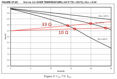
Resistors R10, R14 and R19 are used to limit the current draw from the PIC18F2550. Due to the fact VOH will drop when IOH increase (Figure 8), pin AUX (RA4), pin ICSPCLK (RA3) and pin ICSPDAT (RA2) will all be working within its safe zone.
1.6 PICkit 2 Human Machine Interface
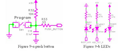
One push button (Figure 9-a) and three LEDs (Figure 9-b) are used in PICkit 2 as human machine interface. A 10K resistor R32 is used as pull-up, when there is no push button action, a logic High will send to PIC18F2550. When the "Program" push button SW1 is pushed, a logic Low will send to PIC18F2550. The push button is used to force PIC18F2550 enter bootloader mode at power-up, or trigger chip programming after power-up. The "POWER" LED will be constantly lit when PICkit 2 is power up. The "TARGET" LED will lit when PICKit 2 supply Vdd to external circuits. The "BUSY" LED will lit when PICkit2 is communicating with PC or programming a chip. Resistors R1, R2, and R3 are used to limit the current to LEDs. For DIY user, it depends the LED type you are using, any resistor between 300 ohm to 1.5K ohm should work. Using smaller value resistor, you got brighter LED but the PICKit 2 will consume more electric current.
1.7 PICkit 2 I2C EEPROM for Programmer-To-Go (PTG) feature
PICkit 2 supports 128K byte of I2C EEPROM and 256K byte of EEPROM. Default is 128K byte of EEPROM, customer can upgrade to 256K byte of EEPROM by replace the 2 pieces of 24LC512 chipsets with 24LC1025. There is some hardware change on pin A2 between 24LC512 and 24LC1025. For DIY user, Figure 10 illustrates a hardware design to be compatible with both 24LC512 and 24LC1025. With 24LC512 on board, R38 and R39 provide pull-down connection. With 24LC1025 on board, R40 and R41 provide pull up connection. 24LC512 and 24LC1025 are exclusive, same it true for the pull-up (R40 and R41) and pull down (R38 and R39) resistors.
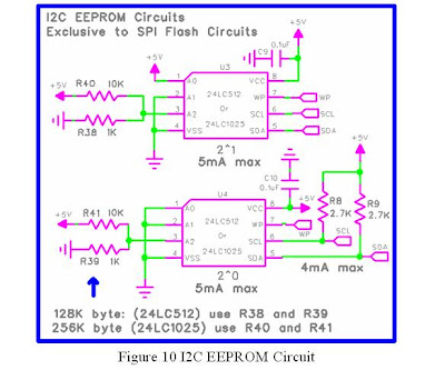
R8 and R9 provide pull up for I2C bus. PIC18F2550 store data to I2C EEPROM by SCL and SDA connection. With the on board EEPROM, the PICKit 2 can program PIC microcontrollers without a PC.
1.8 PICkit 2 ICSP interface
Two types of ICSP interfaces are used in Microchip programmers: RJ12 6p6c connector (Figure 11-a), and 6-pin female header (0.100" spacing) (Figure 11-b). Functionally, they are identical and each has its own pros and cons. The error-proof RJ12 connector using spring contacts to compensate the worn out on pins, it is relatively expensive and takes more space on circuit board. The 6-pin female header takes less circuit board space, but there is limit compensation for pin/contact worn out and there is no mechanism to prevent backwards connection. The RJ12 connector is used in ICD2, ICD3, and RealICE. The 6-pin female header is used in PICKit 2 and PICkit 3. For DIY user, either 6-pin female header or RJ12 connector can be used. For high quality purpose, the RJ12 connector is recommended.
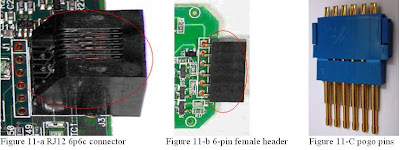
Pogo pin technology (Figure 11-C) can be used to extend the connector life for RJ12 connector and 6-pin header, it is highly recommended for heavy duty usage or manufacturing environment.
The ICSP signal definition on programmer side between the RJ12 6p6c connector and the 6pin female header is opposite. This situation can be easily solved by using different ICSP cables. For ICD2, ICD3, and RealICE, a RJ12 standard cable (Figure 12) is normally used. To be compatible with any circuit board developed for ICD2, a RJ12 reverse cable (Figure 12) can be used with Au Group Electronics developed BB0703 product family.

References:
Special thanks for Walter Kicinski from Microchip Technology Inc. for his constant Support.
1. PICkit 2 Microcontroller Programmer User’s Guide; DS51553E 2/27/2008
2. Au Group Electronics CB0703 Schematic:
http://www.auelectronics.com/Hardware-CB0703.htm
3. http://en.wikipedia.org/wiki/USB
4. Microchip PIC18F2455/2550/4455/4550 Data Sheet
5. Microchip PIC18F2220/2320/4220/4320 Data Sheet, Figure 27-25
6. Google Groups: pickit-devel
Dec. 2008
Au Group Electronics
The Microchip PICkit2 is a USB based ICSP (In Circuit Serial Programming) programmer. Since its first release, Microchip has opened all resource of PICkit2 to the public, which includes all software source code and hardware schematics. With this open-architecture, DIY fans and experts can add hardware features, fix bugs, or modify the source code for operation systems other than Microsoft Windows, e.g. Linux.
PICkit2, MPLAB, ICD2, ICD3, RealICE and PICkit 2 programmer are trademarks of Microchip Technology Inc.
Note: This documents reflect only personal opinions and experiences, it shall not be used for any other purpose other than open-source/education purpose.
Fundamental Design of Microchip PICkit 2
1.1 USB Power Supply and Connection
PICkit 2 is a USB powered device, it gets all the power from PC USB +5V power supply. In default, USB Mini-B connector (Figure 1-a) is used. However, other types of USB connectors can also be used, e.g. USB Type B connector (Figure 1-b).

The USB specification provides a 5 V supply on a single wire from which connected USB devices may draw power. The specification provides for no more than 5.25 V and no less than 4.75 V (5 V±5%) between the positive and negative bus power lines.
A USB "unit load" is defined as 100mA in USB 2.0, and was raised to 150mA in USB 3.0. A maximum of 5 unit loads can be drawn from a port in USB 2.0, and was raised to 6 in USB 3.0. There are two types of devices: low-power and high-power. Low-power devices draw at most 1 unit load, with minimum operating voltage of 4.4V in USB 2.0, and 4V in USB 3.0. High-power devices draw the maximum number of unit loads supported by the standard. All devices default as low-power but the device's software may request high-power as long as the power is available on the providing bus.
The PICkit 2 is a low-power device. Its USB current limit is set at 100mA. When the total current for both target and the PICkit 2 programmer exceeds this current limit, the USB port may turn off. In this case, the target need be powered externally.
Since PICKit 2 itself can draw electrical current as high as 75mA, the current draw for the application circuit should be limited to 25mA if PICkit 2 programmer supplies power. It is always a good practice to use external power when programming hi-performance/power-hungry chipsets, such as: dsPIC30Fs (they normally consume high current when running at high speed).
When a PICkit 2 is used to power application circuit, ensure that the application circuit does not slow the Vdd rise-time to longer than 500 us.
The +5V USB power supply is connected to capacitor C5 and C6 internally (Figure 2-a) for local voltage stability control. A 2.7Kohm resistor R34 was added after the PICKit 2 "red button" revision. R34 is used to bleed capacitor C5 and C6 when a USB connection is off. This helps improving the PICkit 2 HID-recognition performance when it is re-connected to PC in a very short interval.

PIC18F2550 (USB microcontroller) is the soul of the PICkit 2. Two pins (D+ and D-) of PIC18F2550 are used to connect to USB Data+ and Data- from PC (Figure 2-b). All PC application program communicate with PIC18F2550 via these USB D+/D- connection.
An internal 3.3V regulator is used to power the internal transceiver. A 0.47uF capacitor C7 (Figure 2-b) is used to stabilize the 3.3V supply. For PICkit 2 DIY (Do-It-Yourself), the "USB Voltage Regulator" configuration bit for PIC18F2550 must be set as "Enabled" (Figure 3).

1.2 PIC18F2550 ICSP Connection
Like any other PIC microcontroller, the PIC18F2550 is able to be re-programmed even when it is soldered on the printed circuit board. The 5-pin ICSP connection is illustrated in figure 4-a and figure 4-b. This design provides the reprogramming and recovering capability on the chipset whenever there is anything messed up with the PICkit 2 firmware. To reprogram or recover the PIC18F2550 in the PICkit 2, another functional PIC programmer, such as PICkit 2, ICD2, ICD3, RealICE, etc. is needed. It is always a good practice to have at least two PIC programmers, e.g. one ICD2 and one PICkit 2, or two PICKit 2.

PIC18F2550 ICSP Pins
1.3 PICkit 2 ICSP VPP Boost voltage Generation and Control MechanismAs a universal PIC programmer, the VPP signal generation circuit on PICkit 2 must cover all PIC microcontrollers. The VPP voltage requirement varies from 3.3V (dsPIC33F) to 13V (PIC18F); the VPP electrical current specification is normally less than 10mA. PICkit 2 itself runs at 5 volt. Thus, an on-board switch mode boost circuit (Figure 5) is used to generate any voltage higher than target voltage ("+V_TGT" and "VDD_TGT_OUTPUT" (Figure 6-b)).

To stabilize the power supply of the switch mode boost circuit and damp the possible power noise sending back to the main power supply, C13 and C14 is used, and they should be placed as close as possible to inductor L1. The PIC18F2550 controls the switch frequency and dwell time of Q4 (both MMBT2222 (600mA) and MMBT3904 (200mA) can be used.). For DIY user, the capacity for inductor L1 should be at least 10mA. When Q4 is on, electric current flow through L1 and Q4, energy is stored in L1. When Q4 is turned off, a high voltage is generated at pin 2 of L1. The Schottky diode D3 will be on when the induced voltage is higher than the voltage on capacitor C15, electric current will keep flowing through L1 and D3. This will charge the capacitor and raise its voltage to desired VPP voltage. Resistor R22 and R24 generate a feedback signal which is send back to PIC18F2550. With "VPP_FEEDBACK" signal, the PIC18F2550 can then precisely adjust switch frequency and dwell time on Q4. This feedback boost circuit mechanism can generate a voltage higher than "VDD_TGT_OUTPUT". A large value and high voltage rated capacitor should be used as C15. R22 and R24 should use 1% or better accuracy resistor. A Schottky type diode must be used at D3 to secure low voltage drop and power consuming.
R23, R25, R27, Q7 and Q6 are used as ON/OFF switch of VPP. When "VPP_ON" is set high logic by PIC18F2550, Q7 will be on, which will then turn on Q6, the voltage on C15 will appear on PICkit 2 ICSP VPP Pin. When a low logic is send to Q7 by PIC18F2550, Q7 and Q6 will be turned off. This in turn cut off the VPP supply to external circuit. When Q6 and Q8 are both off, the PICkit 2 ICSP VPP Pin is floating. The PIC18F2550 can turn on Q8 and it will clamp PICkit 2 ICSP VPP Pin to ground. This has been used in PICkit 2 self test procedure. The overall VPP control procedure makes it possible to turn on and turn off VPP at any time.
1.4 PICkit 2 ICSP Vdd Generation and Isolation Mechanism
PICkit 2 can provide Vdd to power external circuit or isolate the internal generated Vdd from the external Vdd when external Vdd is detected.
On Figure 6-a, the PIC18F2550 will control the PWM dwell time of "VDD_TGT_ADJ" output, which is integrated by capacitor C8 and resistor R4. A reference voltage is generated at the negative input (U2-pin-3) of a rail to rail operational amplifier U2. R5 and R6 is used to generate voltage feedback to positive input of U2. R7 is used to generate a small electric load and bleed the capacitor (e.g. C11 and C12) when power is turned off. MOSFET Q1 is controlled by U2 in switch mode. When "+V_TGT" is lower than the voltage PIC18F2550 set, feedback voltage on U2-pin-1 is less than voltage on U2-pin-3, the output on U2-pin-4 is Low, MOSFET Q1 will turn on, the "+V_TGT" will increase. When "+V_TGT" increased to high enough to trigger U2-pin-4 to output a High logic, Q1 will be off. When Q1 is off, the "+V_TGT" will stop rising.
Overall, The PIC18F2550 set a target voltage at U2-pin3 by outputting a PWM wave, then the hardware loop of R5, R6, U2-pin-1, U2-pin-4 and Q1 automatically adjust and generate a stable output of "+V_TGT" at all load. This step-down circuit can output a 2.5V to 5V "+V_TGT" for internal and external circuits. For DIY user, U2 must be a rail-to-rail type operational amplifier; and Q1 must be a MOSFET to keep a very low voltage drop.

Capacitor C11 and C12 (Figure 6-b) is used to stable the "+V_TGT" for transient response. U6-Q2 (P) is used to turn on/off "+V_TGT" and isolate "+V_TGT" from "VDD_TGT_OUTPUT". When "VDD_TGT_P" output from PIC18F2550 is High (default), U6-Q2 (P) is off, no internally generated "+V_TGT" will be output to "VDD_TGT_OUTPUT". When "VDD_TGT_P" output from PIC18F2550 changes to Low, U6-Q2 (P) is on, PICKit 2 supplies Vdd to external circuits.
For protection purpose, D4 is also used to isolate internal generated Vdd with external circuit Vdd. This protection mechanism is implemented just in case anyone turns on external power supply while PICkit 2 is supplying power to external circuit. A high current Schottky type diode must be used at D4. Due to the voltage drop on D4, the maximum Vdd after D4 is around 4.8~4.9V when USB supply is 5V. Use other type of diode or small current Schottky type diode at D4 will lead to higher voltage drop. This is critical for some PIC chipset which requires a minimum Vdd 4.6V for good ICSP programming practice (an alternative approach is: always use external Vdd for those PIC chipset).
R12, R13, U6-Q1 (N) and R26 are used to detect external power supply. When the "VDD_TGT_N" output from PIC18F2550 is High logic, U6-Q1 (N) is turned on, the "VDD_TGT_FB" input to PIC18F2550 will read Low if there is no external Vdd exist, otherwise, the "VDD_TGT_FB" will read High. Every time, before connecting PICKit 2 internal Vdd to external circuit, PICkit 2 will automatically detect if external Vdd exist or not, if it does or when status is changed, a warning will be displayed.
Diode D1 and Resistor R17 generate a clamping voltage reference for PICKit 2 PGD PGC and AUX signal. Resistor R17 creates some electric load and make sure there is enough electric current flow through D1. D1 will generate some voltage drop across pin 1 and pin 2, this will compensate the Vbe voltage drop on Q2, Q3 and Q5 (MMBT3906) (Figure 7-a, 7-b, 7-c).
1.5 PICkit 2 ICSP PGD, PGC, AUX Signal Generation and Voltage Clamping Mechanism
Per ICSP definition, the PGC is an output only signal, PGD is a bi-direction signal. The AUX is not used for ICSP, but can be used as bi-direction signal too. Theoretically those three pins can all be used as bi-directional function. However, due to the fact the PIC18F2550 pin RA2 (PGD) and pin RA3 (PGC) are TTL type I/O, pin RA4 (AUX) are ST type I/O. When Vdd is less than 3.6V, any operation involved with RA4 will not function correctly when TTL type input/output logic is needed. This has post some Vdd limit to some 3.3V only 11LC, 24LC EEPROM devices. Au Group Electronics developed 3-in-1 and 2-in-1 mini-labs include level-shift circuits to overcome this design limit.
Besides Programming EEPROMs and PICs, PICKit 2 can also be used as many other purpose, e.g. a Logic Tool, a UART Tool, etc.
As we have seen, the PIC18F2550 itself is working with a +5V supply, it can work directly with any +5V capable target PIC chips.
However there are more and more target PIC chips don't support +5V supply anymore, e.g. some of them can only work with voltage/signal at 3.3V, 2.7V etc.
It is a challenge job to have these PIC chips covered by PICkit 2. This technical challenge has been solved by some simple voltage level clamping technology as shown on Figure 7-a, 7-b, 7-c.

On figure 6-b, a voltage reference "CLAMP_REFERENCE" is generated by diode D1 and Resistor R17. It has been used to control the base (pin 2) on PNP transistor Q2, Q3, and Q5 (MMBT3906, Figure 7-a, 7-b, 7-c). Whenever a PIC18F2550 output a high logic (at pin AUX, ICSPCLK, ICSPDAT), and ICSP Vdd is not +5V, the Q2, Q3 and Q5 will kick-in and clamp the output voltage to Vdd level. Due to the fact there is always a voltage drop Vbe between base and emitter of transistor MMBT3906, a diode D1 is used in figure 6-b to compensate this voltage drop.
Resistors R10, R14 and R19 are used to limit the current draw from the PIC18F2550. Due to the fact VOH will drop when IOH increase (Figure 8), pin AUX (RA4), pin ICSPCLK (RA3) and pin ICSPDAT (RA2) will all be working within its safe zone.

1.6 PICkit 2 Human Machine Interface
One push button (Figure 9-a) and three LEDs (Figure 9-b) are used in PICkit 2 as human machine interface. A 10K resistor R32 is used as pull-up, when there is no push button action, a logic High will send to PIC18F2550. When the "Program" push button SW1 is pushed, a logic Low will send to PIC18F2550. The push button is used to force PIC18F2550 enter bootloader mode at power-up, or trigger chip programming after power-up. The "POWER" LED will be constantly lit when PICkit 2 is power up. The "TARGET" LED will lit when PICKit 2 supply Vdd to external circuits. The "BUSY" LED will lit when PICkit2 is communicating with PC or programming a chip. Resistors R1, R2, and R3 are used to limit the current to LEDs. For DIY user, it depends the LED type you are using, any resistor between 300 ohm to 1.5K ohm should work. Using smaller value resistor, you got brighter LED but the PICKit 2 will consume more electric current.

1.7 PICkit 2 I2C EEPROM for Programmer-To-Go (PTG) feature
PICkit 2 supports 128K byte of I2C EEPROM and 256K byte of EEPROM. Default is 128K byte of EEPROM, customer can upgrade to 256K byte of EEPROM by replace the 2 pieces of 24LC512 chipsets with 24LC1025. There is some hardware change on pin A2 between 24LC512 and 24LC1025. For DIY user, Figure 10 illustrates a hardware design to be compatible with both 24LC512 and 24LC1025. With 24LC512 on board, R38 and R39 provide pull-down connection. With 24LC1025 on board, R40 and R41 provide pull up connection. 24LC512 and 24LC1025 are exclusive, same it true for the pull-up (R40 and R41) and pull down (R38 and R39) resistors.

R8 and R9 provide pull up for I2C bus. PIC18F2550 store data to I2C EEPROM by SCL and SDA connection. With the on board EEPROM, the PICKit 2 can program PIC microcontrollers without a PC.
1.8 PICkit 2 ICSP interface
Two types of ICSP interfaces are used in Microchip programmers: RJ12 6p6c connector (Figure 11-a), and 6-pin female header (0.100" spacing) (Figure 11-b). Functionally, they are identical and each has its own pros and cons. The error-proof RJ12 connector using spring contacts to compensate the worn out on pins, it is relatively expensive and takes more space on circuit board. The 6-pin female header takes less circuit board space, but there is limit compensation for pin/contact worn out and there is no mechanism to prevent backwards connection. The RJ12 connector is used in ICD2, ICD3, and RealICE. The 6-pin female header is used in PICKit 2 and PICkit 3. For DIY user, either 6-pin female header or RJ12 connector can be used. For high quality purpose, the RJ12 connector is recommended.

Pogo pin technology (Figure 11-C) can be used to extend the connector life for RJ12 connector and 6-pin header, it is highly recommended for heavy duty usage or manufacturing environment.
The ICSP signal definition on programmer side between the RJ12 6p6c connector and the 6pin female header is opposite. This situation can be easily solved by using different ICSP cables. For ICD2, ICD3, and RealICE, a RJ12 standard cable (Figure 12) is normally used. To be compatible with any circuit board developed for ICD2, a RJ12 reverse cable (Figure 12) can be used with Au Group Electronics developed BB0703 product family.

References:
Special thanks for Walter Kicinski from Microchip Technology Inc. for his constant Support.
1. PICkit 2 Microcontroller Programmer User’s Guide; DS51553E 2/27/2008
2. Au Group Electronics CB0703 Schematic:
http://www.auelectronics.com/Hardware-CB0703.htm
3. http://en.wikipedia.org/wiki/USB
4. Microchip PIC18F2455/2550/4455/4550 Data Sheet
5. Microchip PIC18F2220/2320/4220/4320 Data Sheet, Figure 27-25
6. Google Groups: pickit-devel
Labels:
BB0703 (PICKit 2)
Thursday, April 23, 2009
How to manually update BB0703(PICkit 2) Operating system?
Author: Chaonan Chen, Huihui Duan, Au Group Electronics
There is very few opportunity ever since the PICkit 2 V2.4x release for a PICkit 2 losing a OS. However it still happens from time to time even in a very very small possibility. When this is happening the PICKit 2 will blink the red LED indicating there is no functioning OS. To get the PICKit 2 back to normal, a new PICkit 2 OS needs be manually downloaded into the PIC18F2550 chipset.
There is very few opportunity ever since the PICkit 2 V2.4x release for a PICkit 2 losing a OS. However it still happens from time to time even in a very very small possibility. When this is happening the PICKit 2 will blink the red LED indicating there is no functioning OS. To get the PICKit 2 back to normal, a new PICkit 2 OS needs be manually downloaded into the PIC18F2550 chipset.
The following tutorial is a step by step guide on how to manually upgrade the PICKit 2 OS. It also answers the following frequent asked question.
Question Asked:
What does it mean when the Busy LED (on PICKit 2) flashes once per second without pushing and holding the button while BB0703 is connected to a USB? How do I correct this?
Answers from Au Group Electronics:
The Busy LED blinking means the unit is in the bootloader mode. For a normal unit, pushing and holding the button while connect BB0703 with USB will manually force the BB0703 (PICkit 2) entering bootloader mode.
To bring the BB0703 (PICkit 2) back to normal programming mode, PICkit 2 Operating System needs to be downloaded from the “PICkit 2 programmer” software. Here is the step by step instruction:
Step 1. Disconnect BB0703 with PC if it was connected before.
Step 2. Open PICkit 2 application software.
Step 3. Connect BB0703 with PC.
Step 4. On "PICKit 2 programmer software", select "Tools-->Check Communication"
"The PICKit 2 has no Operating system. Use the Tools menu to download an OS." will display (figure 1) and the software will be locked up.

Step 5. Disconnect BB0703, this will unfrozen the software.
Step 6. Connect BB0703 back to PC, then click "Tools-->Download PICkit 2 Operating System" (Figure 2)

Step 7. Select the file name "PK2V023200" (assuming V2.61 is used. for other V2.xx, file name should be similar), click OPEN (figure 3)

It will then automatically download the OS into BB0703 (PICKit 2), wait the unit finish the downloading process.

Step 8. Click "Tools-->Check Communication", now it should back to normal mode.

In the V2.5x and V2.6x firmware, there is a self-test safety check feature, if something found wrong on firmware and configuration bits, the unit will be forced entering the bootloader mode thereafter.
A few searches on Microchip Forum provides more background information as the following link.
http://www.microchip.com/forums/tm.aspx?m=297221&mpage=1
It is a good practice to leave the unit on the USB port whenever possible.
Labels:
BB0703 (PICKit 2)
Friday, March 20, 2009
3-in-1 mini-Lab Application Note for dsPIC30F2010
Au Group Electronics
Author: Chaonan Chen, Huihui Duan, Au Group Electronics
This application note use a dsPIC30F2010 (28-pin SDIP package) demonstrate step by step operation on how to use Au Group Electronics "3-in-1 mini-Lab" and "BB0703" to burn program/code into the dsPIC30F microcontroller.
What you need:
Major devices that were used in this application note and their Au Group Electronics part # are listed in table 1.
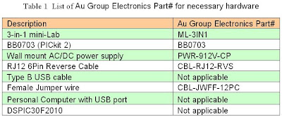
There are two methods to load hex file into target chipset: programming with a PC or Programmer-to-Go. This application note will show both methods.
Program dsPIC30F2010 with a PC:
If hex file has not been burned into BB003 (PICkit 2) programmer, a PC is needed. The hardware setup of Programming with a PC would be similar like figure 1.
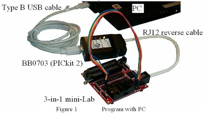
Step 1. Connect 3-in-1 mini-lab, BB0703 with a PC by RJ12 6Pin reverse cable and type B USB cable.
Step 2. Place a piece of dsPIC30F2010 into the 3-in-1 mini-Lab DIP ZIF socket
Note: Only place one chip at a time. E.g. either put a SOIC packaged chipset in SOIC-ZIF socket; or put a DIP packaged chipset in DIP-ZIF socket. Make sure Pin 1 of dsPIC30F2010 agrees with the 1st-pin-mark on circuit board.
Step 3. Use 9 pieces of female jumper wires to connect J1-x to JZ-x on 3-in-1 mini Lab. The position of both ends of the female jump wires are color coded in Table 2.
Note: J1 (J1-1, J1-2, J1-3) are the extension pin headers for RJ12 6P6C connector
JZ-x (JZ-1 to JZ-6) are the extension pin headers for SOIC and DIP ZIF socket.
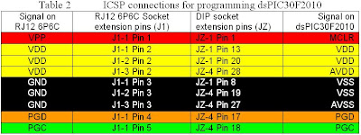
ICSP signal on J1 and dsPIC30F2010 are illustrated in figure 2 for reference

Step 4. Double click shortcut of “PICKit 2 V2.6” to open a "PICkit 2 Programmer", Make sure “PICkit 2 connected, and it’s displayed in the message window, and PIC Device (dsPIC30F2010) found, as shown in figure 3.
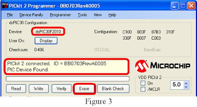
If the device in the ZIF socket are not auto-detect, Click ProgrammerManual Device Select, make sure the checkmark before "Manual Device Select" is gone (picture not show).
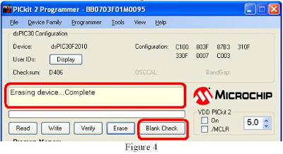
Step 5. Click “Erase” button, as shown in figure 3. Wait a few seconds until “Erasing device … Complete”.
Step 6. Click “Blank Check” button, as shown in figure 4.
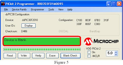
Wait a few seconds, “Device is Blank” will display, as shown in figure 5
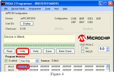
Step 7. Load the hex file, then click “Write” button, as shown in figure 6.
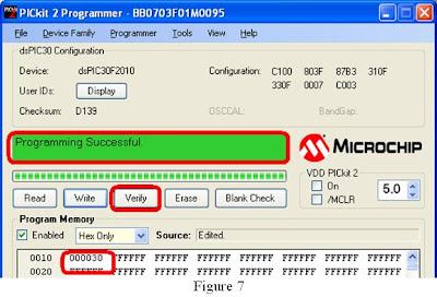
Wait a few seconds, message box will display "Programming Successful", as shown in figure 7
For programming multiple chipsets, Programmer-to-Go will be another convenient and productive solution. It will be demonstrated at the following steps.
Programmer-to-Go (Programming without a PC)
Step 1. Refer to BB0703 (PICkit 2) PTG application note for how to import and download hex file into BB0703 (PICkit 2). After that, PC is not needed for programming microcontroller.
Step 2. Connect the BB0703 with 3-in-1 mini-Lab using a RJ12 reverse cable.
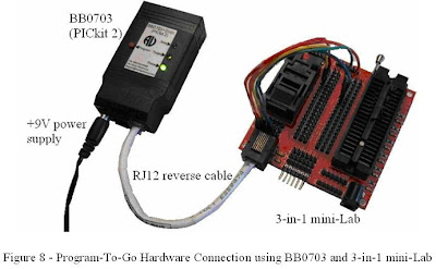
Step 3. Power up BB0703 with +9 V DC supply, as shown in figure 8. The "Target" LED will blink indicating it's ready to program target chip.
Step 4. Load dsPIC30F2010 into ZIF socket.
Step 5. Press "Program" button on BB0703 (PICkit 2), "Busy" LED will be constant on,
Step 6. Wait a few seconds/minutes, until "Busy" LED is off and "Target" LED blink again, which means the hex file has been burned into the target chipset successfully.
Step 7. Repeat steps 4-6 for programming another dsPIC30F2010 chipset
Author: Chaonan Chen, Huihui Duan, Au Group Electronics
This application note use a dsPIC30F2010 (28-pin SDIP package) demonstrate step by step operation on how to use Au Group Electronics "3-in-1 mini-Lab" and "BB0703" to burn program/code into the dsPIC30F microcontroller.
What you need:
Major devices that were used in this application note and their Au Group Electronics part # are listed in table 1.

There are two methods to load hex file into target chipset: programming with a PC or Programmer-to-Go. This application note will show both methods.
Program dsPIC30F2010 with a PC:
If hex file has not been burned into BB003 (PICkit 2) programmer, a PC is needed. The hardware setup of Programming with a PC would be similar like figure 1.

Step 1. Connect 3-in-1 mini-lab, BB0703 with a PC by RJ12 6Pin reverse cable and type B USB cable.
Step 2. Place a piece of dsPIC30F2010 into the 3-in-1 mini-Lab DIP ZIF socket
Note: Only place one chip at a time. E.g. either put a SOIC packaged chipset in SOIC-ZIF socket; or put a DIP packaged chipset in DIP-ZIF socket. Make sure Pin 1 of dsPIC30F2010 agrees with the 1st-pin-mark on circuit board.
Step 3. Use 9 pieces of female jumper wires to connect J1-x to JZ-x on 3-in-1 mini Lab. The position of both ends of the female jump wires are color coded in Table 2.
Note: J1 (J1-1, J1-2, J1-3) are the extension pin headers for RJ12 6P6C connector
JZ-x (JZ-1 to JZ-6) are the extension pin headers for SOIC and DIP ZIF socket.

ICSP signal on J1 and dsPIC30F2010 are illustrated in figure 2 for reference

Step 4. Double click shortcut of “PICKit 2 V2.6” to open a "PICkit 2 Programmer", Make sure “PICkit 2 connected, and it’s displayed in the message window, and PIC Device (dsPIC30F2010) found, as shown in figure 3.

If the device in the ZIF socket are not auto-detect, Click ProgrammerManual Device Select, make sure the checkmark before "Manual Device Select" is gone (picture not show).
Step 5. Click “Erase” button, as shown in figure 3. Wait a few seconds until “Erasing device … Complete”.
Step 6. Click “Blank Check” button, as shown in figure 4.

Wait a few seconds, “Device is Blank” will display, as shown in figure 5

Step 7. Load the hex file, then click “Write” button, as shown in figure 6.

Wait a few seconds, message box will display "Programming Successful", as shown in figure 7

For programming multiple chipsets, Programmer-to-Go will be another convenient and productive solution. It will be demonstrated at the following steps.
Programmer-to-Go (Programming without a PC)
Step 1. Refer to BB0703 (PICkit 2) PTG application note for how to import and download hex file into BB0703 (PICkit 2). After that, PC is not needed for programming microcontroller.
Step 2. Connect the BB0703 with 3-in-1 mini-Lab using a RJ12 reverse cable.
Step 3. Power up BB0703 with +9 V DC supply, as shown in figure 8. The "Target" LED will blink indicating it's ready to program target chip.

Step 4. Load dsPIC30F2010 into ZIF socket.
Step 5. Press "Program" button on BB0703 (PICkit 2), "Busy" LED will be constant on,
Step 6. Wait a few seconds/minutes, until "Busy" LED is off and "Target" LED blink again, which means the hex file has been burned into the target chipset successfully.
Step 7. Repeat steps 4-6 for programming another dsPIC30F2010 chipset
Subscribe to:
Posts (Atom)


